ASU selected as home and partner for CHIPS and Science Act-funded national facility for semiconductor advanced packaging

ASU selected as home and partner for CHIPS and Science Act-funded national facility for semiconductor advanced packaging

by ASU News | Jan 6, 2025 | CHIPS facility, Fall 2024, Industry partnerships, News, Research

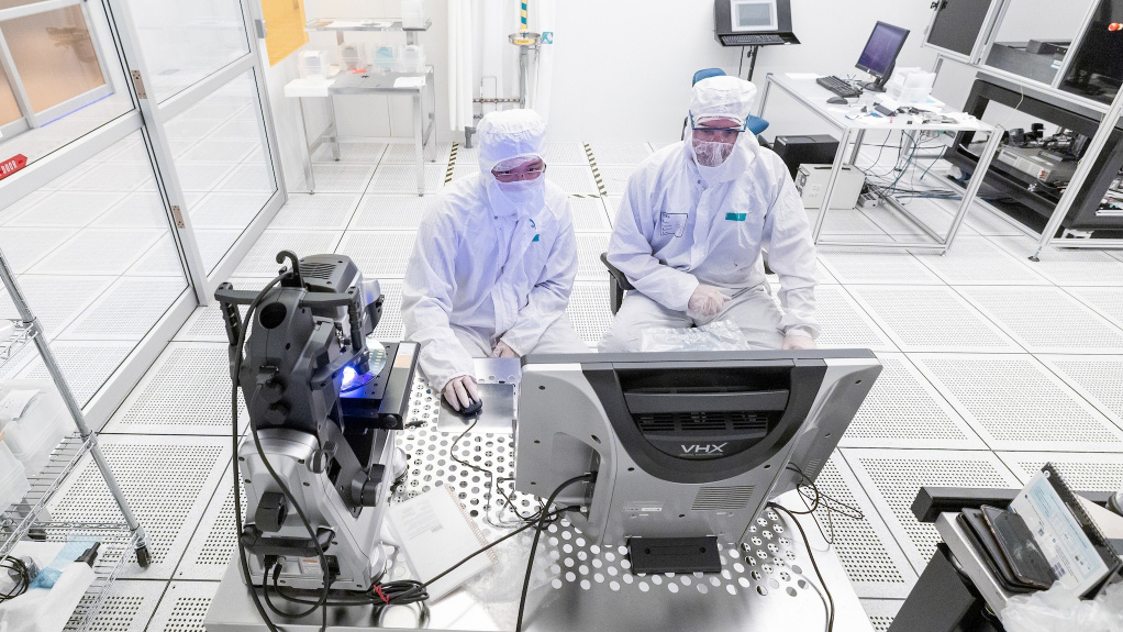
ASU selected as home and partner for CHIPS and Science Act-funded national facility for semiconductor advanced packaging By ASU NewsJanuary 6, 2025 Researchers work inside the clean room area at the MacroTechnology Works facility in the ASU Research Park in Tempe,...

RSS feed: Full Circle: Fulton Engineering news Full Circle: Fulton Engineering news

  • Fulton Schools students attend Foundry School launch in D.C.
  • Where student-athletes, apps and babysitting meet
  • From Discord to campus: How ASU students build community
  • Continuous power for extreme environments
  • Back to school, back to work
Ira A. Fulton Schools of Engineering Logo