NXP Semiconductors partnership to boost manufacturing packaging in Arizona
Investment to fund enhancements at ASU’s MacroTechnology Works facility
By ASU News
December 21, 2023

A new partnership with NXP Semiconductors focused on packaging, an important final step in the manufacturing process, is the latest development in Arizona State University finding new ways to advance Arizona’s expanding semiconductor manufacturing industry.
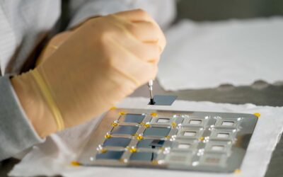
Fueled by the support of the Arizona Commerce Authority and in partnership with NXP, ASU has received a $17.5 million investment to expand and enhance Arizona’s fan-out, wafer-level packaging R&D and workforce training capabilities, and drive the creation of a GaN (gallium nitride) manufacturing and research ecosystem in the state to enable technology of the future and make it available to more companies in the industry.
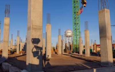
ASU will utilize the funding to purchase equipment to enhance the capabilities of ASU’s MacroTechnology Works in Tempe. The university plans to expand advanced packaging and GaN research to additional capabilities that support 6G, the Internet of Things, machine learning and more.
The expansion will also include student opportunities and workforce development initiatives such as internships and university joint research, and next-gen GaN research development for 6G in partnership with NXP in Chandler.
“The expansion of ASU’s MacroTechnology Works is another important step in enhancing Arizona’s semiconductor ecosystem,” Arizona Gov. Katie Hobbs said. “These new capabilities enable first-of-its-kind training and R&D opportunities to strengthen the state’s workforce and support continued industry growth.”
The state investment goes along with federal investment through the CHIPS and Science Act and significant private sector investment in ASU to enable the university to continue its mission to drive research innovation and the education of the wokers who will fill the jobs that are being created.
“This represents another important step in ASU’s commitment as a university to contribute to advancing America’s domestic semiconductor manufacturing, research and development capabilities,“ ASU President Michael Crow said. “Our recent creation of a Microelectronics Workforce Development Hub and our strategic focus on the university’s MacroTechnology Works facility are both in place to assist with achieving the objectives outlined today and we look forward to working with the Arizona Commerce Authority and NXP to drive success at an accelerated rate.”
Already working in partnership, the agreement deepens the relationship between ASU and NXP.
“We are excited for the opportunity to collaborate with ASU, helping train and develop the engineers of the future, who could one day contribute to the development of critical communications infrastructure benefitting both the state of Arizona and U.S. as a whole,” said Jim Norling, vice president of product management, radio power, at NXP Semiconductors. “This partnership will drive innovation in 6G, taking lab concepts through joint research to full-scale manufacturing.”
The expanded capabilities at MacroTechnology Works in Tempe will support future growth opportunities within Arizona’s semiconductor ecosystem. The ASU expansion also builds on Arizona’s efforts to establish shared semiconductor research and manufacturing facilities that postion the state for additional federal investments through the CHIPS program.
“The partnership will contribute not only to the educational journey of our students, which is our core mission, but also to the success of semiconductor industry leaders and startup companies in Arizona,” said Sally Morton, executive vice president of ASU’s Knowledge Enterprise. “Packaging is the final step in the manufacturing process and it is where some of the greatest innovation comes as we look to increase the capacity and speed of semiconductor chips.”
Investment from the Arizona Commerce Authority is a critical component to providing the infrastructure that will enable all of this to happen.
“This new investment showcases Arizona’s continued commitment to advancing our semiconductor industry,” said Sandra Watson, president and CEO of the Arizona Commerce Authority. “We’re proud to support ASU with this exciting expansion, which will expand the state’s semiconductor supply chain and workforce development efforts while building on strategic efforts to establish an advanced packaging ecosystem in Arizona.”
This investment also drives a segment of the manufacturing process that is newly emerging in Arizona — packaging. It is also the part of the process where much of the innovation occurs as industry works to build smaller and smaller chips with greater sustainability and capacity.
“ASU’s role in this partnership, as with all that we do, is to create, accelerate innovation and broaden access,” said Grace O’Sullivan, ASU’s vice president for corporate engagement and strategic partnerships. “The semiconductor industry has incredibly high capital costs that create barriers to entry for startups and entrepreneurs.
“This is an exciting partnership because what we are doing here with NXP is expanding our core facilities, which are open to the community, and that helps to create an environment for innovators to thrive. The result is a stronger, more vibrant semiconductor ecosystem for the entire state.”
The Arizona Commerce Authority investment is part of a $100 million commitment announced last year to increase semiconductor and microelectronics development in the state. In July, ASU, Applied Materials, Inc, and the Arizona Commerce Authority announced plans to create a world-class shared research, development and prototyping facility, the Materials-to-Fab Center in the university’s MacroTechnology Works building at ASU Research Park. The center, which is supported by a $30 million investment from the Arizona Commerce Authority, will be home to Applied Materials’ Center of Excellence in materials deposition technology.
In September, the Department of Defense announced that Arizona was one of eight regional hubs selected under the Department of Defense Microelectronics Comms program. The Southwest Advanced Prototyping (SWAP) Hub proposal was led by ASU. The SWAP Hub was awarded $39.8 million to advance microelectronics research and development in the focus areas of artificial intelligence hardware, 5G/6G and commercial leap ahead technologies. The hub will help create a GaN and advanced packaging and test ecosystem in Arizona by offering lab-to-fab capabilities, including Department of Defense technical areas.
“This is the future of university research — producing knowledge that is of fundamental value — and Arizona State University is eager to continue making a contribution and educating the students who will ultimately lead this work into the future,” Morton said.
Related Stories

Stabenfeldt elected president of Society For Biomaterials
ASU biomedical engineering professor Sarah Stabenfeldt has been elected president of the Society for Biomaterials
ISTB12 to be major economic boost in region
ASU’s 2025 manufacturing engineering building will be “a showcase of what manufacturing is,” with high-tech labs, classrooms, and makerspaces.
Celebrating an excellent microelectronics professor
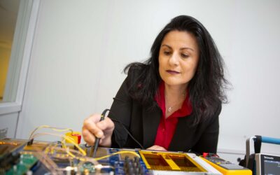
ASU researcher Sule Ozev received the Joseph C. Palais Distinguished Faculty Scholar Award for her innovative research, teaching and service to the ASU community
ASU creates hub of coursework for careers in booming microelectronics industry
ASU’s new Microelectronics Workforce Development Hub offers more than 70 courses for all ages of people wanting to train for a new career.