Making eco-friendly microelectronics
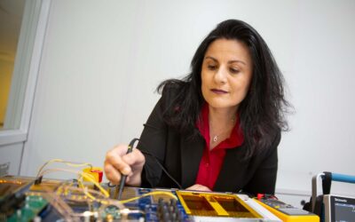
ASU researcher Vidya Chhabria leads research to measure VLSI electronics’ carbon footprint
By TJ Triolo
November 15, 2023

However, the smartphones ubiquitous in pockets worldwide, along with billions of other electronic devices, are on par with or surpassing jet fuel-burning air travel when it comes to contributing to climate change. Researchers at the U.K.’s Lancaster University estimate that computing technology contributes between 2.1% and 3.9% of global greenhouse gas emissions.
As energy-hungry artificial intelligence systems increase in prominence and humanity becomes more dependent on technology, the need for sustainable computing has become more urgent than ever. Vidya Chhabria, an assistant professor of electrical engineering in the Ira A. Fulton Schools of Engineering at Arizona State University, is working to meet that need with her project that measures the lifetime carbon footprint of very large-scale integration, or VLSI, computing systems and design techniques that can make the field more sustainable.
Protecting the future with an eye on VLSI
VLSI systems are electronic chips built using billions of smaller components consisting of wires and transistors, which regulate electricity flow and voltage. VLSI chips are used in electronic devices people use every day, including laptops, smartphones and cameras.
The high number of transistors provides a considerable amount of computing power in a device using VLSI systems. Emerging frontiers in VLSI include 3D and 2.5D systems using heterogeneous integration of chiplets, which refers to combining smaller chips together in one package to form a larger system stacked vertically or horizontally closer than traditional, or monolithic, chips, reducing the area taken up versus one larger chip and enabling the use of even more computing power.
VLSI system development is often aided by electronic design automation, or EDA, which leverages algorithms to enable design and analysis of these systems. While boosting modern electronics’ capabilities, today’s VLSI systems require sizable amounts of energy to be designed, manufactured and run.
VLSI-powered electronics contribute large quantities of greenhouse gas emissions throughout their lives, from when they’re designed and manufactured to their eventual disposal. Chhabria and her collaborators, who include Sarma Vrudhula, a Fulton Schools professor of computer science and engineering in the School of Computing and Augmented Intelligence, and Chetan Choppali Sudarshan, a doctoral student in the School of Electrical, Computer and Energy Engineering, part of the Fulton Schools, seek to measure the carbon footprint of all aspects of a VLSI system.
“To sustain our current use of technology in our daily lives, it’s essential to assess its environmental impact,” Chhabria says. “The idea is to make the semiconductor industry cognizant of the carbon price tag that comes with computing and realize the importance of considering carbon footprint as a first-order metric of optimization in addition to the traditional power, performance, area and cost metrics.”
Estimating environmental impact
Chhabria and her colleagues have designed tools to estimate the carbon footprint of specific VLSI systems using their individual specifications. After system architecture parameters are entered, the tools can calculate the carbon footprint of a VLSI system at the architectural level across its entire lifetime by considering various factors such as system design time, manufacturing process, scaling and yields of chips or chiplets and packaging.
With the information entered, the tools estimate how the combination of parts, system life cycles and manufacturing processes’ individual carbon footprints add up to form a total number.
The tools estimate a carbon footprint number which will enable chip designers and architects to be aware of a VLSI system’s carbon footprint across its lifetime and compare it to other design alternatives. Chhabria and her cohorts have developed one tool already and submitted their findings in a paper accepted for presentation at the Institute of Electrical and Electronics Engineers International Symposium on High-Performance Computer Architecture 2024.
The researchers analyzed different VLSI systems using the tool and found that heterogeneous 2.5D and 3D systems leveraging a predesigned library of chiplets had a lower carbon footprint compared to traditional monolithic chips. Chiplet-based 2.5D and 3D systems have a lower environmental impact by enabling larger yields, enabling mix-and-match design combinations of chiplets in different manufacturing process technologies and allowing the reuse of existing chip designs.
“This is the key time to look at the environmental impact of 2.5D and 3D systems,” Chhabria says. “EDA tools that are used to design these new 2.5D and 3D systems are not yet fully developed to support heterogeneous systems. Because they’re still in their nascent stage, now is the right time to make EDA tools also consider carbon footprint as a metric of optimization.”
The researchers are continuing to develop additional tools that consider more metrics such as chips’ lifespans, power required for operation, number of manufactured parts, the time it takes from design to commercialization and more.
“The hope is for the public and chip design community to take notice of the impact the information and computing technology industry has on the environment and increase the lifetime of their electronic devices,” Chhabria says. “It might involve a straightforward act, such as retaining a fully functional smartphone instead of discarding it simply because a newer model has been launched.”
A potential wide-ranging impact and future applications
For Sudarshan, a newer member of the VLSI research community, the paper represents the first research work he has had published.
“Our work is open-source and available on GitHub, contributing to the community’s efforts to advance this field and demonstrate the significance of sustainable architecture designs in reducing VLSI’s overall carbon footprint,” he says.
Chhabria is working with Aman Arora, an assistant professor of computer science and engineering in the Fulton Schools, to apply the carbon footprint measurement tools to field-programmable gate arrays, or FPGAs, a type of chip with flexible capabilities that can be reprogrammed for a variety of applications.
If successful, the programmability of FPGAs and their potential to serve as sustainable computing alternatives would provide another solution to improve computing’s carbon footprint. The researchers are working on a proposal to gain funding for the work, and Arora is looking for more students interested in sustainable computing.
“If you look at projections of the carbon footprint from computing, it’s going to increase rapidly in the future,” he says. “In one home today, there are probably 50 devices that are running AI workloads. If we can make computing more sustainable by reducing the carbon footprint of the chips we use, that will have a big impact on the ecology of Earth.”
Fulton
Researchers
Vidya Chhabria
Assistant Professor
School of Electrical, Computer and Energy Engineering
Aman Arora
Assistant Professor
School of Computing and Augmented Intelligence
Related Stories

Stabenfeldt elected president of Society For Biomaterials
ASU biomedical engineering professor Sarah Stabenfeldt has been elected president of the Society for Biomaterials

ISTB12 to be major economic boost in region
ASU’s 2025 manufacturing engineering building will be “a showcase of what manufacturing is,” with high-tech labs, classrooms, and makerspaces.
Celebrating an excellent microelectronics professor
ASU researcher Sule Ozev received the Joseph C. Palais Distinguished Faculty Scholar Award for her innovative research, teaching and service to the ASU community

ASU creates hub of coursework for careers in booming microelectronics industry
ASU’s new Microelectronics Workforce Development Hub offers more than 70 courses for all ages of people wanting to train for a new career.